お客様のニーズに合わせ、有機EL(OLED)・液晶ディスプレイ(LCD)に最適なガラス選定と成膜加工、超高精細パターニング加工の対応を致します。
To satisfy our customer’s needs, we select the optimum glass for Organic Light-Emitting-Diode (OLED) and liquid crystal display (LCD), and we offer film coating and high-precision patterning.

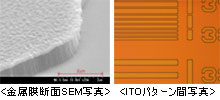
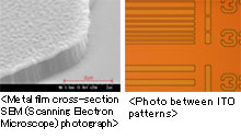
- 電極用ITO膜パターニング〜CF用2nd ITOパターニング
- BMおよび補助電極用各種メタル膜(アルミ(AL)系、クロム(Cr)系、銀(Ag)系、その他の金属膜)の高精細パターニング
- 積層膜パターニング(FFS構造、OLED積層膜)
- LCD用PS、OC形成、OLED用絶縁膜形成、その他有機膜形成
- MEMS加工によるCVD成膜+ドライエッチング各種(SiN、SiO2他)

- 最小線間
- サブミクロン(MEMS)サイズからお客様のご要望により対応させていただきます。10mmx10mm程度〜200mmφ(200mmφ以上は、要相談)
- 対応膜
- サイズからお客様のご要望により対応させていただきます。10mmx10mm程度〜200mmφ(200mmφ以上は、要相談)
ITO、Cr、Ag系、AL系、Si系マザーガラスサイズ〜550×670mmサイズ適用板厚
(総厚)0.2t〜

- 静電容量タッチパネル基板
- FFS、IPS、PSA液晶評価用基板
- MEMSラインを用いた微細加工(ドライエッチング装置を用いた酸化物の微細加工品他)
- OLED用積層膜(無機膜、有機膜の積層化)の評価基板
- 薄膜太陽電池用積層膜(無機膜、有機膜の積層化)の評価基板

- Patterning ITO (Indium Tin Oxide) film for electrodes, patterning 2nd ITO for CF.
- Precision patterning of BM and various metallic films [aluminum (AL), chrome (Cr), and silver (Ag) families] for auxiliary electrodes.
- Patterning multilayer films(for Fringe Field Switching,for OLED) Organic Solar Cell (OPV) )
- Photo Spacer for LCD Insulator for OLED and more(ex.making Organic Films )
- SiN,SiO2 Patterning By CVD and Dry Etching in MEMS Proccessing

- The minimum distance between traces
- We can handle customer's requirement at the sub-micron (MEMS: Micro Electro Mechanical Systems) level and smaller.
10 mm x10 mm to 200 mm φ (For 200 mm φ and above, consultation required)
- Applicable film types
- ITO, Cr, Ag, AL, and Si families
- Mother glass size
- Up to 550x670 mm
- Applicable plate thickness (layer thickness)
- 0.2mm and up

- Capacitance touch panel substrates
- FFS (Fringe Field Switching) mode liquid crystal evaluation board
- Fine processing using an MEMS line
- Multilayer Films(Organic and Inorganic films) for evaluation
工程フロー
| 基板洗浄 |
⇒ |
レジスト
塗布 |
⇒ |
露光 |
⇒ |
現像 |
⇒ |
 |
| |
| エッチング |
⇒ |
レジスト
剥離 |
⇒ |
最終洗浄 |
⇒ |
検査 |
|
Process flow
| Cleaning substrates |
⇒ |
Resist application |
⇒ |
Exposure |
⇒ |
Development |
⇒ |
 |
| |
| Etching |
⇒ |
Resist removal |
⇒ |
Final cleaning |
⇒ |
Inspection |
|